Wednesday, May 5, 2021

AUTOMATIC EMERGENCY LOW POWER LIGHT

 AUTOMATIC EMERGENCY LOW POWER LIGHT

101% working  project hello  friends  today I am gonna  telling  you  about  some  easy  and valuable  electronics projects for  school and  college  practical

Here is a white LED based emergency light that provides the following benefits:

  1.  It is extremely bright due to the use of white LED.
  2. The light turns on automatically when the main supply fails and it turns off when the mains power  resumes.
  3.  When the battery is fully charged then it has its own battery charger, charging stops automatically.

 The circuit comprises  two sections: the charger power supply and the LED driver. The charger power supply is built around section 3 - terminal adjustable regulator IC LM317 (ICI), while the LED driver section is built around transistor BD140 (T2).In the charger power supply section,  input AC mains are moved down by the transformer X1 to deliver 9V, 500 mA to the bridge rectifier, which comprises diodes D1  through D4 . Filter capacitor C1 eliminates ripples.

 Unregulated DC voltage is fed to input pin 3 of IC1 and provides charging  current through diode D5 and limiting resistor R16.  By adjusting preset VR1, the output voltage can be adjusted to deliver the required charging current when the battery gets charged to 6.8V, zener diode ZDI conducts and charging current from regulator ICI finds a path through transistor T1 to ground and it stops charging  of the battery The LED driver section uses a to tal of twelve 10mm white LEDs. 
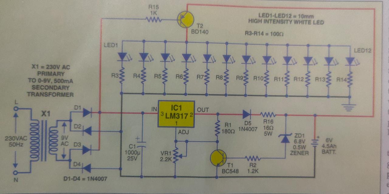
fig1 circuit diagram

 All the LEDs are connected in parallel with a 100 - ohm resistor in series with each.  The common - anode junction of all the twelve LEDs is connected to the collector of pnp transistor T2 and the emitter of transistor T2 is directly connected to the positive terminal of 6V battery.  The unregulated DC voltage, produced at the cathode junction of diodes D1 and D3 is fed to the base of transistor T2 through a 1 kilo - ohm resistor when mains power is available, the base of transistor T2 remains high and T2 does not conduct.  Thus LEDs are off . On the other hand , when mains fails , the base of transistor T2 becomes low and it conducts .

 This makes all the LEDs ( LED1 through LED12 ) glow . The mains power supply , when available , charges the battery and keeps the LEDs off as transistor T2 remains cut - off . During mains failure , the charging section stops working and the battery supply makes the LEDs glow 

Assemble the circuit on a general - purpose PCB and enclose in a cabinet with enough space for battery and switches . Mount the LEDs on the cabinet such that they light up the room . A hole in the cabinet should be drilled to connect 230V AC input for the primary of the transformer .more projects


friends please LIKE  ,SHARE and  FOLLOW    thanks for your support


Tuesday, May 4, 2021

BATTERY LEVEL MONITOR

             BATTERY LAVEL INDICATOR

 101% working  project hello  friends  today I am gonna  telling  you  about  some  easy  and valuable  electronics projects for  school and  college  practical ,

 This general- purpose 12V battery -level indicator  is build around the ubiquitous LED driver IC LM3914. It can check the  voltage level of any battery having output  voltage between 3V and 12V . 
The battery level is display in bar mode. When battery voltage is up to 12V ,LED1 through LED7 glow. similarly, when battery voltage is around 10.50V , LED1 through LED6 glow. A total of ten LEDs are used in this circuit . The battery under test power the  circuit .No addition power supply is required for this tester.

You can test up to 15V battery with this circuit  as it  has ten LEDs with  this circuit  as  it  has  ten  LEDs. The first nine LEDs 1 TO 9 will  glow  when  the battery  under test has 15V output .

 the  potential divider  comprising resistor R4 and R5 provides  reference input  signal  for IC2 at pin 5 . The visual indicator range depend  on the internal reference voltage of IC2 plus value of resistor R6 and preset VR1.With the components values used here the circuit  display between 3V(LED1) and 16.5V(LED10). 


In addition, a push-to read  arrangement  has been realised using popular timer IC LM555(IC1). IC1 is pressed momentarily of when the power is switched  on initially. Its output pin 3 goes high for about five seconds and transistor T1 conducts to provide positive supply at the common anode of LEDs.  This power supply is also ex tended to emitters of transistors T2 and T3 for activating the buzzer.  The LEDs up to the supply level of battery re main lit for the time duration of timer IC1 wired monostable multivibrator.  R2 and C2 determine the time period of the monostable multivibrator .
The circuit bunt around transistors and T3 sounds an alarm when the battery level goes low.  The audio alarm for the battery level can be decided by connecting the base of transistor T2 to a particular pin of IC2.  For example, if you want an alarm when the battery level goes to low 9V, connect the base of transistor T2 to pin 15 of IC2.  You will observe LED5 switching off and an alarm sounds.

Assemble the circuit on a  multi PCB and breadboard .  Before en closing the circuit in a box, calibrate the various voltage levels.  For calibration, connect the 15V variable regulated power supply and initially set it at 3V.  Press switch S1 and slowly adjust VR1 until LED1 lights up.  Similarly, increase the input voltage to 15V in steps of 1.5V.  Press switch S1 and slowly adjust VR1 until the corresponding LED (LED2 through LED9) lights up Re - check your calibration and when sure of its correctness, paint - lock preset VR1 and remove the variable power supply.  Now your battery - level monitor is ready for use!


friends please LIKE  ,SHARE and  FOLLOW    thanks for your support

Monday, May 3, 2021

MOBILE PHONE DETECTOR

        MOBILE PHONE  DETECTOR 

 101% working  project hello  friends  today I am gonna  telling  you  about  some  easy  and valuable  electronics projects for  school and  college  practical , 


This handy, pocket-size mobile transmission detector can sense the presence of an activated mobile phone from a distance of one and-a-half meters. So it can be used to prevent use of mobile phones in examination halls, confidential rooms, etc. It is also useful for detecting the use of mobile phone for spying and unauthorized video transmission.

 The circuit can detect both the in-coming and outgoing calls, SMS and video transmission even if the mobile phone is kept in the silent mode. The moment the bug detects RF transmission signal from an activated mobile phone, it starts sounding a beep alarm and the LED blinks. The alarm continues until the signal transmission ceases.

 An ordinary RF detector using tuned LC circuits is not suitable for detecting signals in the GHz frequency band used in mobile phones. The transmission frequency of mobile phones ranges from 0.9 to 3 GHz with a wavelength of 3.3 to 10 cm. So a circuit detecting gigahertz signals is required for a mobile phone detector .

 Here the circuit uses a 0.22µF disk capacitor (C3) to capture the RF signals from the mobile phone. The lead length of the capacitor is fixed as 18 mm with a spacing of 8 mm between the leads to get the desired frequency. The disk capacitor along with the leads acts as a small gigahertz loop antenna to collect the RF signals from the mobile phone. Op-amp IC CA3130 (IC1) is used in the circuit as a current-to-voltage converter with capacitor C3 connected between its inverting and non-inverting inputs. It is a CMOS version using gate-protected p-channel MOSFET transistors in the input to provide very high input impedance, very low input current and very high speed of performance. The output CMOS transistor is capable of swinging the output volt
age to within 10 mV of either supply voltage terminal.


 Capacitor C3 in conjunction with the lead inductance acts as a transmission line that intercepts the signals from the mobile phone. This capacitor creates a field, stores energy and transfers the stored energy in the form of minute current to the inputs of IC1. This will upset the balanced input of ICI and convert the current into the corresponding output voltage.

Capacitor C4 along with high-value resistor R1 keeps the non-inverting in- put stable for easy swing of the out- put to high state. Resistor R2 provides the discharge path for capacitor C4. Feedback resistor R3 makes the inverting input high when the output becomes high. Capacitor C5 (47pF) is connected across 'strobe' (pin 8) and 'null' inputs (pin 1) of IC1 for phase compensation and gain control to optimize  frequency response.

 When the mobile phone signal is detected by C3, the output of IC1 becomes high and low alternately  according to the frequency of the signal as indicated by LED1. This triggers monostable timer IC2 through capacitor C7. Capacitor C6 maintains the base bias of transistor T1 for fast switching action. The low-value timing components R6 and C9 produce very short time delay to avoid audio nuisance. 

Assemble the circuit on a general- purpose PCB as compact as possible and enclose in a small box like junk mobile case. As mentioned earlier, capacitor C3 should have a lead length of 18 mm with lead spacing of 8 mm. Carefully solder the capacitor in standing position with equal spacing of the leads. The response can be optimized by trimming the lead length of C3 for the desired frequency. You may use a short telescopic type antenna. Use the miniature 12V battery of a remote control and a small buzzer to make the gadget pocket-size. The unit will give the warning indication if someone uses mobile phone within a radius of 1.5 meters.

more projects 


friends please LIKE  ,SHARE and  FOLLOW    thanks for your support


SENSITIVE TOUCH SECURITY ALARM

     SENSITIVE  TOUCH  SECURITY ALARM 

 101% working  project hello  friends  today I am gonna  telling  you  about  some  easy  and valuable  electronics projects for  school and  college  practical , 

This alarm circuit is frequency- operated. It uses an NE567 phase-locked loop to sense a particular frequency band. We all know that AC mains line frequency is 50 Hz. Radiation signals from mains wiring can travel a few meters distance. These can induce an electromagnetic field in the human body also.
 So when you touch a metallic object, 50HZ signals from your body (induced from mains wiring) will be injected into it. These can be amplified and fed to a PLL circuit tuned to 50 Hz.

Fig1 -SENSITIVE  TOUCH SECURITY ALARM Circuit Diagram 

Fig. 1 shows the circuit of the hum- sensitive touch alarm, while Fig. 2 shows the power supply circuit required to operate the touch alarm. Here, popular operational amplifier HA741 is used as the signal amplifier. The amplified signals are fed to NE567 PLL circuit.

 If the input frequency is 50 Hz, the output of PLL goes low and activates the electrical circuit of LED1 and buzzer. LED1 glows and at the same time the piezobuzzer sounds. Adjust preset VR1 for correct operation. Use a small touch plate at the input of op-amp IC1.
 Connect the touch plate to the input circuit of op-IC1 using a shielded cable. Keep amp the length of the shielded cable as short as possible to avoid losses to already feeble induced signal.
Fig2- power supply circuit diagram

 If you use a battery, keep the unit near AC mains wiring for generating 50HZ signal through induction. Use of a half-wave rectifier power supply is recommended for this circuit. The reason: The output of the half-wave rectifier is 50 Hz as against the 100HZ pulsating ripple of the full-wave rectifier and it will also serve the purpose of inducing 50HZ signal.


friends please LIKE  ,SHARE and  FOLLOW    thanks for your support   


Sunday, May 2, 2021

IR DETECTOR

                         IR DETECTOR

hello  friends  today I am gonna  telling  you  about  some  easy  and valuable  electronics projects 
for  school and  college  practical 


Using this IR detector, you can check the functioning of remote handsets. It can also be used as the front end of IR-based receiver circuits. The detector uses photovoltaic property of the IR diode to detect IR radiations in the range of 30 cm to 50 cm.
HOME MADE IR DETECTOR 

The gallium-arsenide p-n junction diode (IR1) can generate around 100µA current when exposed to a source of visible or infrared light. The current thus generated is proportional to the intensity of light falling on it. In the circuit, diode IR1 detects IR radiations and generates corresponding current,

which is amplified by a current-to-voltage converter built around IC TL071 (1C1), which is a low-noise JFET op-amp with low input voltage. The input offset current of TL071 is 2 nA and the input bias current is 7 nA. The non-inverting input of IC1 is connected to a potential divider comprising R1 and R2. High- value resistor R1 along with capacitor Cl keeps the non-inverting input stable for easy swing of output to high state.
IR DETECTOR CIRCUIT  DIAGRAM 

 Infrared detector diode IR1 is connected between the non-inverting and inverting input  cathode toward  the inverting  input. resistor R3 perform  the negative feedback function.
 when the power is switched on through switch SI, LEDI lights up to indicate that the circuit is ready. It, however, gradually turns off as resistor R3 draws current from the output. The circuit then goes to the standby mode and maintains balance between the non-inverting and inverting inputs. At this stage, the output will remain low and LEDI 'off

. When the remote control handset is focused towards the detector diode and any of the buttons is pressed, the IR beam falls on IR1 to generate a cur- rent, which upsets the balance between non-inverting and inverting inputs of IC1. LEDI starts flashing to indicate the presence of IR beam that was coming from the remote handset.

 Assemble the circuit on a general- purpose PCB and enclose in a suitable cabinet. Use a 9V PP3 battery to power the circuit. Black tubing is necessary for the IR diode since daylight may affect the functioning of the circuit.

friends please LIKE  ,SHARE and  FOLLOW    thanks for your support   

ULTRASONIC SOUND BEAM BULGRAL ALARM

            ULTRASONIC SOUND BEAM BULGER  ALARM

hello  friends  today I am gonna  telling  you  about  some  easy  and valuable  electronics projects 
for  school and  college  practical  

This unique burglar alarm makes use of the invisible, inaudible ultrasonic sound beam to detect movements. Ultrasonic transducers operate at maximum efficiency when driven at 40kHz frequency. So an ultrasonic transmitter and receiver pair operating at 40 kHz is used to control the buzzer or the relay The transmitter unit is built around CMOS IC CD4001 (see Fig. 1).

fig1-TRANSMITTER CIRCUIT 

 By adjusting the 22-kilo-ohm preset (VR1), the oscillator frequency can be set to approximately 40 kHz. The ultrasonic transmitter transducer is driven by two complementary buffer stages of CD4001 and its current drain is very low
.
 The receiver unit uses a two- stage 40kHz preamplifier followed by switching circuit, buzzer driver, etc (see Fig. 2).
Fig2-receiver circuit 


 Adjust VR2 in the receiver circuit till the buzzer stops sounding while the receiver senses ultrasonic sound from the transmitter. When the ultrasonic beam is interrupted by the movement of a person or any other object crossing its path, NPN transistor T1 stops conducting and transistor T5 conducts. It activates the buzzer and LED1 for three to four seconds. This duration depends on the time taken by 470uF capacitor (C8) connected at the base of transistor T5 to discharge fully through resistor R13.

 The burglar alarm duration can be set to a desired value with the values of C8 and R13. The alarm circuit comprising transmitter, receiver and associated circuits operates off a 9-12V regulated power supply. The receiver circuit requires regulated 12V.

 You can also use un- regulated power supply here. Assemble the transmitter and receiver circuits on separate general- purpose PCBS. Align the ultrasonic transducer such that the signal falls directly on the ultrasonic receiver. The piezo buzzer (Pz1) can be replaced with a relay to control the mains-operated alarm.

friends please LIKE  ,SHARE and  FOLLOW    thanks for your support   

Saturday, May 1, 2021

USB POWER BOOSTER

                          USB POWER BOOSTER

hello  friends  today I am gonna  telling  you  about  some  easy  and valuable  electronics projects 
for  school and  college  practical  


The USB serial  bus can be  configured for connecting several peripheral device to a single PC. It is more complex that RS232 ,but faster and simpler for expansion .

since a PC  can supply only  a limited power to the external devices connected  through its USB port ,When too many device  are connected  simultaneously ,there is a possibility  of power  shortage. therefore an external power source has to be  added to power the external device .


In  USB , two  different type of connectors are used type A  and type B. The  circuit presented here is an addon unit , designed  to add more power to a  USB  supply line (type-A ). when  power  signal  from the PC (+5V ) is received through socket A ,LED1  glows, opto-diac  IC1 conduct and TRIAC1 is triggered, resulting in availability of main supply  from the primary  of transformer X1 deliver 12V at its secondary, which is rectified by a bridge rectified  comprising diode D1 through D4 and filtered by capacitor C2.

Regulator IC 7805 is used to stabilise the rectified DC .Capacitor C3 at the output of the regulator  bypassed the ripples present in the rectified  DC output. LED1 indicates the status of the  USB power booster circuit .
circuit diagram  of the USB power booster

Assemble the circuit on a general purpose PCB and enclose in a suitable  cabinet. Bring out the +5V, ground and data point in the type-A socket connected the data cables as assigned in the circuit  and the USB power booster is ready to function 

friends please like ,share  and comment   thanks for your support   


ELECTRONIC CALCULATOR

               ELECTRONIC CALCULATOR hello  friends  today I am gonna  telling  you  about  some  easy  and valuable  electronics projects  ...